Shift4

question

Build a 4-bit shift register (right shift), with asynchronous reset, synchronous load, and enable.

  • areset: Resets shift register to zero.
  • load: Loads shift register with data[3:0] instead of shifting.
  • ena: Shift right (q[3] becomes zero, q[0] is shifted out and disappears).
  • q: The contents of the shift register.

If both the load and ena inputs are asserted (1), the load input has higher priority.

Module Declaration

1
2
3
4
5
6
7
module top_module(
input clk,
input areset, // async active-high reset to zero
input load,
input ena,
input [3:0] data,
output reg [3:0] q);

solution

1
2
3
4
5
6
7
8
9
10
11
12
13
14
15
16
17
18
19
20
21
22
23
24
25
26
27
28
29
30
31
32
33
34
35
36
37
38
39
40
41
42
43
44
45
46
47
48
49
50
51
52
// my answer
module top_module(
input clk,
input areset, // async active-high reset to zero
input load,
input ena,
input [3:0] data,
output reg [3:0] q);
always @(posedge clk or posedge areset) begin
if (areset) begin
q <= 0;
end
else if (load == 1'b1) begin
q <= data;
end
else begin
if (ena == 1'b1) begin
q[3] <= 0;
q[2] <= q[3];
q[1] <= q[2];
q[0] <= q[1];
// q <= q[3:1];
end
end
end
endmodule

// reference answer
module top_module(
input clk,
input areset,
input load,
input ena,
input [3:0] data,
output reg [3:0] q);

// Asynchronous reset: Notice the sensitivity list.
// The shift register has four modes:
// reset
// load
// enable shift
// idle -- preserve q (i.e., DFFs)
always @(posedge clk, posedge areset) begin
if (areset) // reset
q <= 0;
else if (load) // load
q <= data;
else if (ena) // shift is enabled
q <= q[3:1]; // Use vector part select to express a shift.
end

endmodule

Rotate100

question

Build a 100-bit left/right rotator, with synchronous load and left/right enable. A rotator shifts-in the shifted-out bit from the other end of the register, unlike a shifter that discards the shifted-out bit and shifts in a zero. If enabled, a rotator rotates the bits around and does not modify/discard them.

  • load: Loads shift register with data[99:0] instead of rotating.

  • ena[1:0]

    : Chooses whether and which direction to rotate.

    • 2'b01 rotates right by one bit
    • 2'b10 rotates left by one bit
    • 2'b00 and 2'b11 do not rotate.
  • q: The contents of the rotator.

Module Declaration

1
2
3
4
5
6
module top_module(
input clk,
input load,
input [1:0] ena,
input [99:0] data,
output reg [99:0] q);

solution

1
2
3
4
5
6
7
8
9
10
11
12
13
14
15
16
17
18
19
20
21
22
23
24
25
26
27
28
29
30
31
32
33
34
35
36
37
38
39
40
41
42
43
44
45
46
47
48
49
50
51
52
53
54
// my ans
module top_module(
input clk,
input load,
input [1:0] ena,
input [99:0] data,
output reg [99:0] q);
always @(posedge clk) begin
if (load) begin
q <= data;
end
else begin
case (ena)
2'b01: begin
q[98:0] <= q[99:1];
q[99] <= q[0];
// q <= {q[0], q[99:1]};
end
2'b10: begin
q[99:1] <= q[98:0];
q[0] <= q[99];
// q <= {q[98:0], q[99]};
end
default:
q <= q;
endcase
end
end
endmodule

// ref ans
module top_module(
input clk,
input load,
input [1:0] ena,
input [99:0] data,
output reg [99:0] q);

// This rotator has 4 modes:
// load
// rotate left
// rotate right
// do nothing
// I used vector part-select and concatenation to express a rotation.
// Edge-sensitive always block: Use non-blocking assignments.
always @(posedge clk) begin
if (load) // Load
q <= data;
else if (ena == 2'h1) // Rotate right
q <= {q[0], q[99:1]};
else if (ena == 2'h2) // Rotate left
q <= {q[98:0], q[99]};
end
endmodule

debug

  • case 里面对应的一个情况超过了一个语句描述,则需要用begin end

Shift18-Arithmetic Shift Register

question

Build a 64-bit arithmetic shift register, with synchronous load. The shifter can shift both left and right, and by 1 or 8 bit positions, selected by amount.

An arithmetic right shift shifts in the sign bit of the number in the shift register (q[63] in this case) instead of zero as done by a logical right shift. Another way of thinking about an arithmetic right shift is that it assumes the number being shifted is signed and preserves the sign, so that arithmetic right shift divides a signed number by a power of two.

There is no difference between logical and arithmetic left shifts.

  • load: Loads shift register with data[63:0] instead of shifting.

  • ena: Chooses whether to shift.

  • amount

    : Chooses which direction and how much to shift.

    • 2'b00: shift left by 1 bit.
    • 2'b01: shift left by 8 bits.
    • 2'b10: shift right by 1 bit.
    • 2'b11: shift right by 8 bits.
  • q: The contents of the shifter.

Module Declaration

1
2
3
4
5
6
7
module top_module(
input clk,
input load,
input ena,
input [1:0] amount,
input [63:0] data,
output reg [63:0] q);

Hint…

A 5-bit number 11000 arithmetic right-shifted by 1 is 11100, while a logical right shift would produce 01100.

Similarly, a 5-bit number 01000 arithmetic right-shifted by 1 is 00100, and a logical right shift would produce the same result, because the original number was non-negative.

solution

1
2
3
4
5
6
7
8
9
10
11
12
13
14
15
16
17
18
19
20
21
22
23
24
25
26
27
28
29
30
31
32
33
module top_module(
input clk,
input load,
input ena,
input [1:0] amount,
input [63:0] data,
output reg [63:0] q);
always @(posedge clk) begin
if (load) begin
q <= data;
end
else begin
if (ena) begin
case (amount)
2'b00: begin
q <= {q[62:0],1'b0};
end
2'b01: begin
q <= {q[55:0],8'b0};
end
2'b10: begin
q <= q[63] ? {1'b1,q[63:1]} : {1'b0,q[63:1]};
end
2'b11: begin
q <= q[63] ? {8'hff,q[63:8]} : {8'h00,q[63:8]};
end
default:
q <= q;
endcase
end
end
end
endmodule

debug

  • 三元运算符语法错误:正确:q <= q[63] ? {1'b1,q[63:1]} : {1'b0,q[63:1]};;错误:q[63] ? q <= {1'b1,q[63:1]} : q <= {1'b0,q[63:1]};
  • case 的对象错误:R:amount;E:ena。
  • case 的参数错误:R:2’b10;E:10。

LFSR

A linear feedback shift register is a shift register usually with a few XOR gates to produce the next state of the shift register. A Galois LFSR is one particular arrangement where bit positions with a “tap” are XORed with the output bit to produce its next value, while bit positions without a tap shift. If the taps positions are carefully chosen, the LFSR can be made to be “maximum-length”. A maximum-length LFSR of n bits cycles through 2n-1 states before repeating (the all-zero state is never reached).

The following diagram shows a 5-bit maximal-length Galois LFSR with taps at bit positions 5 and 3. (Tap positions are usually numbered starting from 1). Note that I drew the XOR gate at position 5 for consistency, but one of the XOR gate inputs is 0.

Lfsr5.png

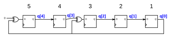
Build this LFSR. The reset should reset the LFSR to 1.

Module Declaration

1
2
3
4
5
module top_module(
input clk,
input reset, // Active-high synchronous reset to 5'h1
output [4:0] q
);

Hint…

The first few states starting at 1 are 00001, 10100, 01010, 00101, … The LFSR should cycle through 31 states before returning to 00001.

solution

1
2
3
4
5
6
7
8
9
10
11
12
13
14
15
16
17
18
19
20
21
22
23
24
25
26
27
28
29
30
31
32
33
34
35
36
37
38
39
40
41
42
43
44
45
46
47
48
49
50
51
52
53
// my answer
module top_module(
input clk,
input reset, // Active-high synchronous reset to 5'h1
output [4:0] q
);
always @(posedge clk) begin
if (reset) begin
q <= 5'h1;
end
else begin
q[4] <= q[0];
q[3] <= q[4];
q[2] <= q[3] ^ q[0];
q[1] <= q[2];
q[0] <= q[1];
end
end
endmodule

// ref answer
module top_module(
input clk,
input reset,
output reg [4:0] q);

reg [4:0] q_next; // q_next is not a register

// Convenience: Create a combinational block of logic that computes
// what the next value should be. For shorter code, I first shift
// all of the values and then override the two bit positions that have taps.
// A logic synthesizer creates a circuit that behaves as if the code were
// executed sequentially, so later assignments override earlier ones.
// Combinational always block: Use blocking assignments.
always @(*) begin
q_next = q[4:1]; // Shift all the bits. This is incorrect for q_next[4] and q_next[2]
q_next[4] = q[0]; // Give q_next[4] and q_next[2] their correct assignments
q_next[2] = q[3] ^ q[0];
end


// This is just a set of DFFs. I chose to compute the connections between the
// DFFs above in its own combinational always block, but you can combine them if you wish.
// You'll get the same circuit either way.
// Edge-triggered always block: Use non-blocking assignments.
always @(posedge clk) begin
if (reset)
q <= 5'h1;
else
q <= q_next;
end

endmodule

summary

这里的作者使用了状态机的写法,通过组合逻辑列出其下一状态的值,这里需要注意的是,组合逻辑使用的是阻塞赋值,后一个值将前一个值覆盖,电路里将直接忽略前一个时刻的值。

Mt2015 lfsr

question

Taken from 2015 midterm question 5. See also the first part of this question: mt2015_muxdff

Mt2015 muxdff.png

Write the Verilog code for this sequential circuit (Submodules are ok, but the top-level must be named top_module). Assume that you are going to implement the circuit on the DE1-SoC board. Connect the R inputs to the SW switches, connect Clock to KEY[0], and L to KEY[1]. Connect the Q outputs to the red lights LEDR.

Module Declaration

1
2
3
4
module top_module (
input [2:0] SW, // R
input [1:0] KEY, // L and clk
output [2:0] LEDR); // Q

Hint…

This circuit is an example of a Linear Feedback Shift Register (LFSR). A maximum-period LFSR can be used to generate pseudorandom numbers, as it cycles through 2n-1 combinations before repeating. The all-zeros combination does not appear in this sequence.

solution

1
2
3
4
5
6
7
8
9
10
11
12
13
14
15
16
module top_module (
input [2:0] SW, // R
input [1:0] KEY, // L and clk
output [2:0] LEDR); // Q
reg [2:0] next_ledr;
always @(*) begin
next_ledr = {LEDR[1] ^ LEDR[2],LEDR[0],LEDR[2]} ;
end
always @(posedge KEY[0]) begin
if (KEY[1])
LEDR <= SW;
else begin
LEDR <= next_ledr;
end
end
endmodule

Lfsr32

See Lfsr5 for explanations.

Build a 32-bit Galois LFSR with taps at bit positions 32, 22, 2, and 1.

Module Declaration

1
2
3
4
5
module top_module(
input clk,
input reset, // Active-high synchronous reset to 32'h1
output [31:0] q
);

solution

1
2
3
4
5
6
7
8
9
10
11
12
13
14
15
16
17
18
19
20
21
22
module top_module(
input clk,
input reset, // Active-high synchronous reset to 32'h1
output [31:0] q
);
wire [31:0] next_q;
always @(*) begin
next_q = {q[0],q[31:1]};
next_q[31] = q[0];
next_q[21] = q[22] ^ q[0];
next_q[1] = q[2] ^ q[0];
next_q[0] = q[1] ^ q[0];
end
always @(posedge clk) begin
if (reset) begin
q <= 32'h1;
end
else begin
q <= next_q;
end
end
endmodule

Exams/m2014 q4k

question

Implement the following circuit:

Exams m2014q4k.png

Module Declaration

1
2
3
4
5
module top_module (
input clk,
input resetn, // synchronous reset
input in,
output out);

solution

1
2
3
4
5
6
7
8
9
10
11
12
13
14
15
16
17
18
19
20
module top_module (
input clk,
input resetn, // synchronous reset
input in,
output out);
reg [3:0] q;
assign out = q[3];
always @(posedge clk) begin
if (!resetn) begin
q <= 0;
end
else begin
integer i;
for (i = 0; i <= 2; i = i + 1) begin
q[i + 1] <= q[i];
end
q[0] <= in;
end
end
endmodule

Exams/2014 q4b

question

Consider the n-bit shift register circuit shown below:

Exams 2014q4.png

Write a top-level Verilog module (named top_module) for the shift register, assuming that n = 4. Instantiate four copies of your MUXDFF subcircuit in your top-level module. Assume that you are going to implement the circuit on the DE2 board.

  • Connect the R inputs to the SW switches,
  • clk to KEY[0],
  • E to KEY[1],
  • L to KEY[2], and
  • w to KEY[3].
  • Connect the outputs to the red lights LEDR[3:0].

(Reuse your MUXDFF from exams/2014_q4a.)

Module Declaration

1
2
3
4
5
module top_module (
input [3:0] SW,
input [3:0] KEY,
output [3:0] LEDR
);

solution

1
2
3
4
5
6
7
8
9
10
11
12
13
14
15
16
17
18
19
20
21
22
23
24
25
26
27
28
29
30
31
32
33
34
35
36
37
38
39
40
41
42
43
module top_module (
input [3:0] SW,
input [3:0] KEY,
output [3:0] LEDR
); //
genvar i;
generate
for (i = 3; i >= 1 ; i = i - 1) begin: for_bk
MUXDFF MUXDFF_inst(
.w(LEDR[i]),
.R(SW[i - 1]),
.E(KEY[1]),
.L(KEY[2]),
.clk(KEY[0]),
.Q(LEDR[i - 1])
);
end
MUXDFF MUXDFF_inst_3(
.w(KEY[3]),
.R(SW[3]),
.E(KEY[1]),
.L(KEY[2]),
.clk(KEY[0]),
.Q(LEDR[3])
);
endgenerate

endmodule

module MUXDFF (
input w, R, E, L,
input clk,
output Q
);
wire mid, next_Q;
always @(*) begin
next_Q = L ? R : mid;
mid = E ? w : Q;
end
always @(posedge clk) begin
Q <= next_Q;
end
endmodule

Exams/ece241 2013q12

question

In this question, you will design a circuit for an 8x1 memory, where writing to the memory is accomplished by shifting-in bits, and reading is “random access”, as in a typical RAM. You will then use the circuit to realize a 3-input logic function.

First, create an 8-bit shift register with 8 D-type flip-flops. Label the flip-flop outputs from Q[0]…Q[7]. The shift register input should be called S, which feeds the input of Q[0] (MSB is shifted in first). The enable input controls whether to shift. Then, extend the circuit to have 3 additional inputs A,B,C and an output Z. The circuit’s behaviour should be as follows: when ABC is 000, Z=Q[0], when ABC is 001, Z=Q[1], and so on. Your circuit should contain ONLY the 8-bit shift register, and multiplexers. (Aside: this circuit is called a 3-input look-up-table (LUT)).

Module Declaration

1
2
3
4
5
6
module top_module (
input clk,
input enable,
input S,
input A, B, C,
output Z );

solution

1
2
3
4
5
6
7
8
9
10
11
12
13
14
15
16
17
18
19
20
21
22
23
24
25
26
27
28
29
30
31
32
33
34
35
36
37
38
39
40
41
42
43
44
45
46
47
48
49
50
51
52
53
54
55
56
module top_module (
input clk,
input enable,
input S,
input A, B, C,
output Z );
reg [7:0] Q;
always @(posedge clk) begin
if (enable) begin
for (integer i = 0; i < 7 ; i = i + 1) begin
Q[i + 1] <= Q[i];
end
Q[0] <= S;
end
end
module top_module (
input clk,
input enable,
input S,
input A, B, C,
output Z );
reg [7:0] Q;
always @(posedge clk) begin
if (enable) begin
for (integer i = 0; i < 7 ; i = i + 1) begin
Q[i + 1] <= Q[i];
end
Q[0] <= S;
end
end
always @(*) begin
case ({A,B,C})
3'b000: Z = Q[0];
3'b001: Z = Q[1];
3'b010: Z = Q[2];
3'b011: Z = Q[3];
3'b100: Z = Q[4];
3'b101: Z = Q[5];
3'b110: Z = Q[6];
3'b111: Z = Q[7];
endcase
end
endmodule
/* always @(*) begin
case {A,B,C}: // USAGE OF CASE IS WRONG
3'b000: Z = Q[0];
3'b001: Z = Q[1];
3'b010: Z = Q[2];
3'b011: Z = Q[3];
3'b100: Z = Q[4];
3'b101: Z = Q[5];
3'b110: Z = Q[6];
3'b111: Z = Q[7];
endcase
end
*/

Debug

  • 注意case的用法