【Verilog学习】-08-时序逻辑-基础触发器
1.DFF
Create a single D flip-flop.
1 | module top_module ( |
2.DFF8
Create 8 D flip-flops. All DFFs should be triggered by the positive edge of clk.
1 | module top_module ( |
3.Dff8r
Create 8 D flip-flops with active high synchronous reset. All DFFs should be triggered by the positive edge of clk.
1 | module top_module ( |
4.Dff8p
Create 8 D flip-flops with active high synchronous reset. The flip-flops must be reset to 0x34 rather than zero. All DFFs should be triggered by the negative edge of clk.
1 | module top_module ( |
5.Dff8ar
Create 8 D flip-flops with active high asynchronous reset. All DFFs should be triggered by the positive edge of clk.^1
1 | module top_module ( |
6.Dff16e
Create 16 D flip-flops. It’s sometimes useful to only modify parts of a group of flip-flops. The byte-enable inputs control whether each byte of the 16 registers should be written to on that cycle. byteena[1] controls the upper byte d[15:8], while byteena[0] controls the lower byte d[7:0].
resetn is a synchronous(同步的,不要和异步高反了, active-low reset.
All DFFs should be triggered by the positive edge of clk.
1 | module top_module ( |
7.D Latch
Implement the following circuit:

Note that this is a latch, so a Quartus warning about having inferred a latch is expected.
1 | module top_module ( |
8.DFF with gate
Implement the following circuit:

1 | module top_module ( |
9.DFF + MUX - 0
Taken from ECE253 2015 midterm question 5
Consider the sequential circuit below:

Assume that you want to implement hierarchical Verilog code for this circuit, using three instantiations of a submodule that has a flip-flop and multiplexer in it. Write a Verilog module (containing one flip-flop and multiplexer) named top_module for this submodule.
1 | module top_module ( |
10.DFF + MUX - 1
Consider the n-bit shift register circuit shown below:

Write a Verilog module named top_module for one stage of this circuit, including both the flip-flop and multiplexers.
1 | module top_module ( |
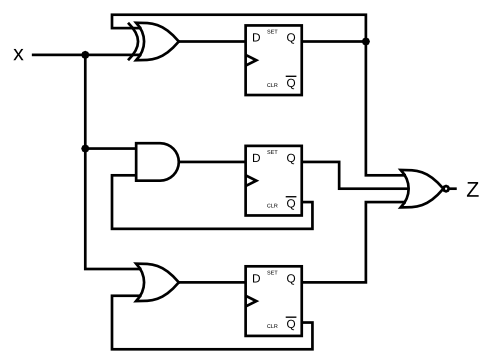
11.DFF + GATES
Given the finite state machine circuit as shown, assume that the D flip-flops are initially reset to zero before the machine begins.
Build this circuit.
Hint: Be careful with the reset state. Ensure that each D flip-flop’s Q output is really the inverse of its Q output, even before the first clock edge of the simulation.
1 | module top_module ( |
12.JK-FF[^2]
A JK flip-flop has the below truth table. Implement a JK flip-flop with only a D-type flip-flop and gates. Note: Qold is the output of the D flip-flop before the positive clock edge.
| J | K | Q |
|---|---|---|
| 0 | 0 | Qold |
| 0 | 1 | 0 |
| 1 | 0 | 1 |
| 1 | 1 | ~Qold |
1 | module top_module ( |
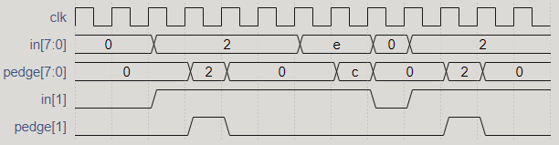
13.Edge Detect
For each bit in an 8-bit vector, detect when the input signal changes from 0 in one clock cycle to 1 the next (similar to positive edge detection). The output bit should be set the cycle after a 0 to 1 transition occurs.
Here are some examples. For clarity, in[1] and pedge[1] are shown separately.
1 | module top_module ( |
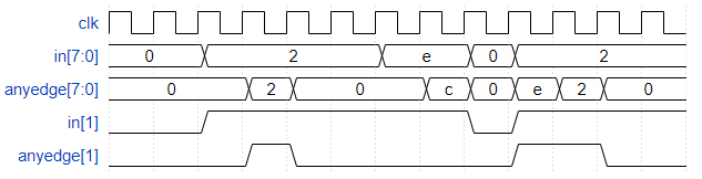
14.EdgeDetect2
For each bit in an 8-bit vector, detect when the input signal changes from one clock cycle to the next (detect any edge). The output bit should be set the cycle after a 0 to 1 transition occurs.
Here are some examples. For clarity, in[1] and anyedge[1] are shown separately.
1 | module top_module ( |
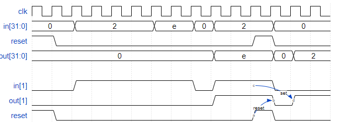
15.EdgeCapture
For each bit in a 32-bit vector, capture when the input signal changes from 1 in one clock cycle to 0 the next. “Capture” means that the output will remain 1 until the register is reset (synchronous reset).
Each output bit behaves like a SR flip-flop: The output bit should be set (to 1) the cycle after a 1 to 0 transition occurs. The output bit should be reset (to 0) at the positive clock edge when reset is high. If both of the above events occur at the same time, reset has precedence. In the last 4 cycles of the example waveform below, the ‘reset’ event occurs one cycle earlier than the ‘set’ event, so there is no conflict here.
In the example waveform below, reset, in[1] and out[1] are shown again separately for clarity.
(注意这里的题意是捕捉下降沿)
1 | module top_module ( |
16.Dualedge
You’re familiar with flip-flops that are triggered on the positive edge of the clock, or negative edge of the clock. A dual-edge triggered flip-flop is triggered on both edges of the clock. However, FPGAs don’t have dual-edge triggered flip-flops, and always @(posedge clk or negedge clk) is not accepted as a legal sensitivity list.
Build a circuit that functionally behaves like a dual-edge triggered flip-flop:
1 | module top_module ( |
标答:
1 | module top_module( |
总结
从13题开始,解题出现了困难。
13、14题的结题思路是一致的,关键点是明白要进行边沿检测,就应该将前一时刻和当前时刻的输入作比较,如果两个输入不同则是出现了边沿。
15题主要是理解题意的问题,要进行下边沿的捕捉,因此需要边沿的检测和锁存,检测的思路和13、14相同,而锁存的方式是通过if语句。
16题是双边沿检测的问题,这里是涉及到一个双边沿检测电路的代码综合的问题[^3]。注意具体的实现方法。
参考资料
[^2]: 通过仿真和综合认识JK触发器(Verilog HDL语言描述JK触发器)_Reborn Lee-CSDN博客_jk触发器verilog代码
[^3]: verilog实现双边沿触发器Dual-edge triggered flip-flop_城外南风起的博客-CSDN博客_verilog 双边沿